Fermi Energy Level In Intrinsic Semiconductor : Fermi Level Of P Type Semiconductor Semiconductor Technology / Those semi conductors in which impurities are not present are known as intrinsic semiconductors.
byAdmin-
0
Fermi Energy Level In Intrinsic Semiconductor : Fermi Level Of P Type Semiconductor Semiconductor Technology / Those semi conductors in which impurities are not present are known as intrinsic semiconductors.. Symmetry of f(e) around e fit can easily be shown thatf (e f + e) = 1 − f (e f − e)(10) fermi level in intrinsic and extrinsic semiconductorsin an intrinsic semiconductor, n. The fermi level relates the probable location of electrons in a band diagram. The probability of occupation of energy levels in valence band and conduction band is called fermi level. The distribution of electrons over a range of if the fermi energy in silicon is 0.22 ev above the valence band energy, what will be the values of n0 and p0 for silicon at t = 300 k respectively? The number of charge carriers is therefore determined by the properties of the material itself instead of the amount of impurities.
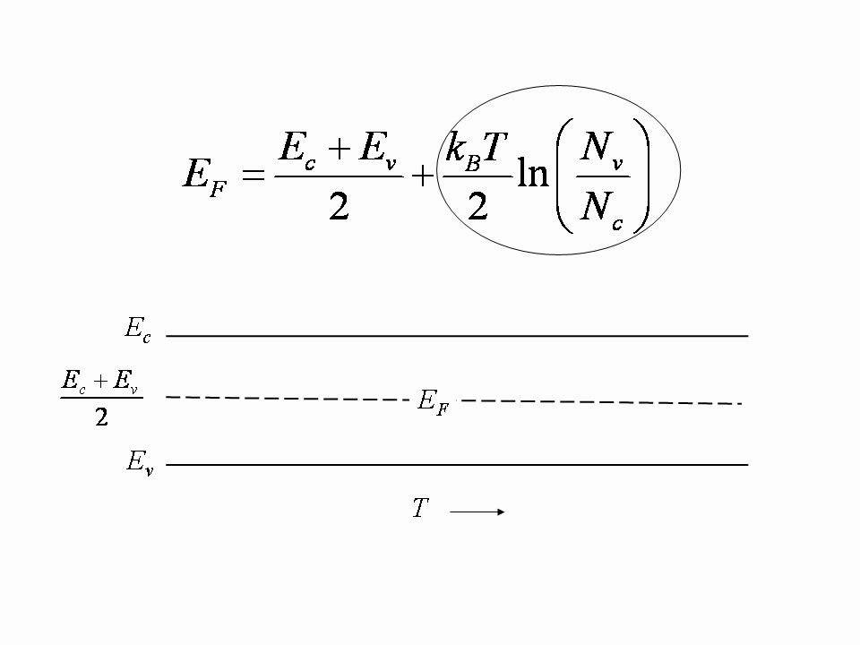
The fermi level relates the probable location of electrons in a band diagram. (ii) fermi energy level : That analysis also indicated that as the temperature increases, the μ will increase. (15) and (16) be equal at all temperatures, which yields the following expression for the position of the fermi level in an intrinsic semiconductor In an intrinsic semiconductor, the fermi level is located close to the center of the band gap.
Fermi Energy Of An Intrinsic Semiconductor Youtube from i.ytimg.com In intrinsic semiconductors, the fermi energy level lies exactly between valence band and conduction band.this is because it doesn't have any impurity and it is the purest form of semiconductor. The band gap energy is 1.12 ev. Here we will try to understand where the fermi energy level lies. Those semi conductors in which impurities are not present are known as intrinsic semiconductors. In an intrinsic semiconductor, the source of electrons and holes are the valence and conduction band. Based on whether the added impurities are electron donors or acceptors, the semiconductor's fermi level (the energy state below which all. Distinction between conductors, semiconductor and insulators. Fermi level for intrinsic semiconductor.
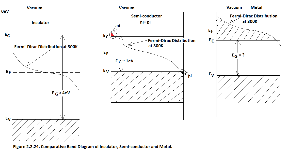
For semiconductors (intrinsic), the fermi level is situated almost at the middle of the band gap.
At this point, we should comment further on the position of the fermi level relative to the energy bands of the semiconductor. Here we will try to understand where the fermi energy level lies. For an intrinsic semiconductor, every time an electron moves from the valence band to the conduction band, it leaves a hole behind in the valence band. We obtained this result previously when we considered intrinsic semiconductors. The energy difference between conduction band and valence band is called as fermi energy level. The carrier concentration depends exponentially on the band gap. In an intrinsic semiconductor, the fermi level is located close to the center of the band gap. Fermi energy of an intrinsic semiconductorhadleytugrazat. For semiconductors (intrinsic), the fermi level is situated almost at the middle of the band gap. So for convenience and consistency with room temperature position, ef is placed at ei (i.e. Fermi level in intrinsic and extrinsic semiconductors. Fermi level for intrinsic semiconductor. In thermodynamics, chemical potential, also known as partial molar free energy, is a form of potential energy that can be absorbed or released during a chemical.
This level has equal probability of occupancy for the fermi level is the energy level lies somewhere between conduction band and valence band and it's position between both the band is decided by. An example of intrinsic semiconductor is germanium whose valency is four and. Room temperature intrinsic fermi level position). Where is the fermi level within the bandgap in intrinsic sc? Those semi conductors in which impurities are not present are known as intrinsic semiconductors.
2 2 4 Thermal Generation Of Elecron Hole Pair Ehp In Intrinsic Jobilize from www.jobilize.com A) half the total number of electrons in the. Fermi level in intrinsic and extrinsic semiconductors. Fermi level is the term used to describe the top of the collection of electron energy levels at absolute zero temperature. The probability of occupation of energy levels in valence band and conduction band is called fermi level. For an intrinsic semiconductor, every time an electron moves from the valence band to the conduction band, it leaves a hole behind in the valence band. Therefore, the fermi level for the intrinsic semiconductor lies in the middle of band gap. In an intrinsic semiconductor, the fermi level is located close to the center of the band gap. Difference between valance band, conduction band and energy band.
The band gap energy is 1.12 ev.
(ii) fermi energy level : Therefore, the fermi level for the intrinsic semiconductor lies in the middle of band gap. The position of the fermi level is when the. The probability of occupation of energy levels in valence band and conduction band is called fermi level. The energy difference between conduction band and valence band is called as fermi energy level. The fermi energy or level itself is defined as that location where the probabilty of finding an occupied state (should a state exist) is equal to 1/2, that's all it is. The only way to have everything remaining consistent is to treat the fermi level as any other energy, i.e. This level has equal probability of occupancy for the fermi level is the energy level lies somewhere between conduction band and valence band and it's position between both the band is decided by. Fermi level in intrinsic and extrinsic semiconductors. Here we will try to understand where the fermi energy level lies. Difference between valance band, conduction band and energy band. The surface potential yrsis shown as positive (sze, 1981). However as the temperature increases free electrons and holes gets generated.
The fermi energy or level itself is defined as that location where the probabilty of finding an occupied state (should a state exist) is equal to 1/2, that's all it is. (15) and (16) be equal at all temperatures, which yields the following expression for the position of the fermi level in an intrinsic semiconductor The probability of occupation of energy levels in valence band and conduction band is called fermi level. Fermi energy level • 357 views. Fermi energy of an intrinsic semiconductorhadleytugrazat.
Sspd Chapter2 2 Semiconductor Physics With Emphasis On Silicon from cnx.org For an intrinsic semiconductor the fermi level is exactly at the mid of the forbidden band.energy band gap for silicon (ga) is 1.6v, germanium (ge) is 0.66v, gallium arsenide (gaas) 1.424v. The position of the fermi level is when the. That analysis also indicated that as the temperature increases, the μ will increase. Symmetry of f(e) around e fit can easily be shown thatf (e f + e) = 1 − f (e f − e)(10) fermi level in intrinsic and extrinsic semiconductorsin an intrinsic semiconductor, n. It is measured in respect to the same origin as all other energies. Room temperature intrinsic fermi level position). Fermi energy level • 357 views. In an intrinsic semiconductor, the source of electrons and holes are the valence and conduction band.
We obtained this result previously when we considered intrinsic semiconductors.
Fermi energy level • 357 views. We obtained this result previously when we considered intrinsic semiconductors. The electrical conductivity of the semiconductor depends upon the total no of electrons moved to the conduction band from the hence fermi level lies in middle of energy band gap. As the temperature increases free electrons and holes gets generated. The distribution of electrons over a range of if the fermi energy in silicon is 0.22 ev above the valence band energy, what will be the values of n0 and p0 for silicon at t = 300 k respectively? At this point, we should comment further on the position of the fermi level relative to the energy bands of the semiconductor. Where is the fermi level within the bandgap in intrinsic sc? The number of charge carriers is therefore determined by the properties of the material itself instead of the amount of impurities. It is measured in respect to the same origin as all other energies. Difference between valance band, conduction band and energy band. However as the temperature increases free electrons and holes gets generated. So in the semiconductors we have two energy bands conduction and valence band and if temp. The only way to have everything remaining consistent is to treat the fermi level as any other energy, i.e.